Monday, November 14th 2022

AMD Explains the Economics Behind Chiplets for GPUs
AMD, in its technical presentation for the new Radeon RX 7900 series "Navi 31" GPU, gave us an elaborate explanation on why it had to take the chiplets route for high-end GPUs, devices that are far more complex than CPUs. The company also enlightened us on what sets chiplet-based packages apart from classic multi-chip modules (MCMs). An MCM is a package that consists of multiple independent devices sharing a fiberglass substrate.
An example of an MCM would be a mobile Intel Core processor, in which the CPU die and the PCH die share a substrate. Here, the CPU and the PCH are independent pieces of silicon that can otherwise exist on their own packages (as they do on the desktop platform), but have been paired together on a single substrate to minimize PCB footprint, which is precious on a mobile platform. A chiplet-based device is one where a substrate is made up of multiple dies that cannot otherwise independently exist on their own packages without an impact on inter-die bandwidth or latency. They are essentially what should have been components on a monolithic die, but disintegrated into separate dies built on different semiconductor foundry nodes, with a purely cost-driven motive.

 AMD's pivot to chiplets is driven by rising costs of semiconductor wafers, as the silicon fabrication process advances along the transistor-size scale. Although AMD became a fabless company 13 years ago, it had a cozy arrangement with Globalfoundries, the former AMD foundry division that it spun off. The company continued to source processors from Globalfoundries until the 14 nm-12 nm class FinFET nodes, and although Globalfoundries had originally planned to make a sub-10 nm node that was competitive with TSMC 7 nm and Samsung 8 nm; these plans fell through. AMD maintained relations with TSMC, from which it was manufacturing its Radeon GPUs. Since TSMC had the best 7 nm-class node and the capacity to scale production upward; the company made its biggest bet, building processors on 7 nm.
AMD is hardly TSMC's only customer, and the company soon realized that it couldn't make high core-count CPUs on monolithic 7 nm dies; nor could it do what it did with EPYC "Naples," which were basically "4P on a stick" MCMs, with wasted die-space to redundant components. It hence disintegrated the processor. The components that could benefit the most from the shrink to 7 nm; the CPU cores, would be built on tiny dies containing 8 CPU cores each, which the company would call CPU complex dies (CCDs). The smaller the die, the higher the yield per wafer, and so the company decided that a 80 mm²-ish piece of silicon with 8 CPU cores, would talk to a separate die containing all the components that it could afford to build on a slightly older node with minimal impact on the product's overall power/thermal characteristics. It would call this the I/O die. AMD would go on to build both client Ryzen and server EPYC products with this approach, as the 8-core CCDs were common to both product lines. The client desktop processor would have a smaller I/O die suitable to the platform, which it would call cIOD (client I/O die), while the server part, with the ability to connect with a higher number of CCDs, would be called the sIOD (server I/O die). AMD continued to source I/O dies from Globalfoundries, on its 12 nm node, for the past three years. With the latest Ryzen 7000 and 4th Gen EPYC processors based on "Zen 4," AMD is building the CCDs on the 5 nm EUV node, while the I/O dies are built on the less advanced 6 nm node.
Fast forward, and AMD found itself staring at a problem with its Radeon GPUs. The company doesn't make as much money selling discrete GPUs as it does with CPUs (client+server), so the imperative to reduce manufacturing costs is even higher, without losing competitiveness against NVIDIA. With the GeForce "Ada Lovelace," generation, NVIDIA continues to bet on monolithic silicon for GPU, building even its largest "AD102" chip as a classic monolithic GPU. This presents AMD with an opportunity to lower the manufacturing cost of its GPUs, which could enable it to wage price-wars against NVIDIA, in an attempt to gain market-share. A case in point is the relatively aggressive pricing AMD is using for the Radeon RX 7900 XTX, at $999; and the RX 7900 XT at $899, which the company thinks have what it takes to take the fight to NVIDIA's $1,199 RTX 4080 and probably even trade blows with the $1,599 RTX 4090 in some best-case scenarios.
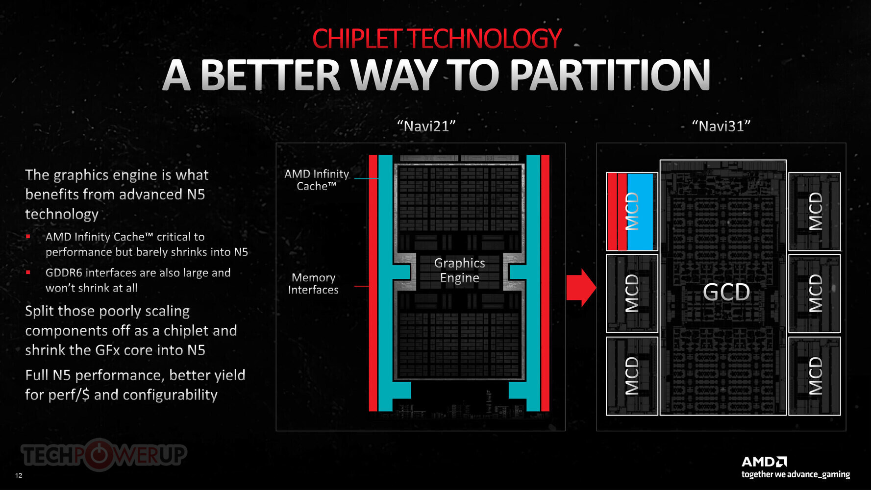
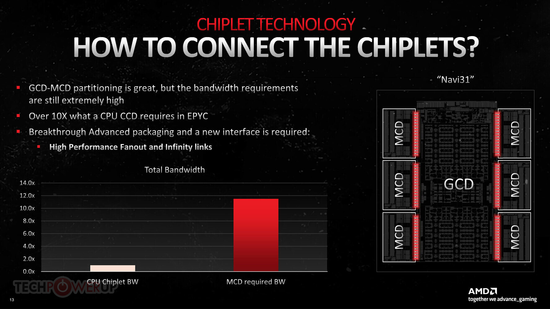
Step one of disintegrating a high-end GPU without hurting its performance, frame-times, and power/thermal characteristics; is to identify the specific components on the silicon that could be spun off into chiplets, that can make do with an older foundry node. For an EPYC server processor, even with 9-12 chiplets, the company only has to deal with hundreds of signal paths traversing the substrate, to interconnect the chiplets. A high-end discrete GPU is a lot more complex, and the scale of these inter-chiplet signal paths number in the thousands (in case of the older "Navi 21" RDNA2 silicon). With the larger "Navi 31" RDNA3, this count is only going to be higher. The company identified the components that made up at least one-third of the die-area that wouldn't benefit tangibly from the switch to 5 nm EUV—these would be the GDDR6 memory controllers, memory PHY, and the Infinity Cache memory (the GPU's L3 cache shared among all Shader Engines).
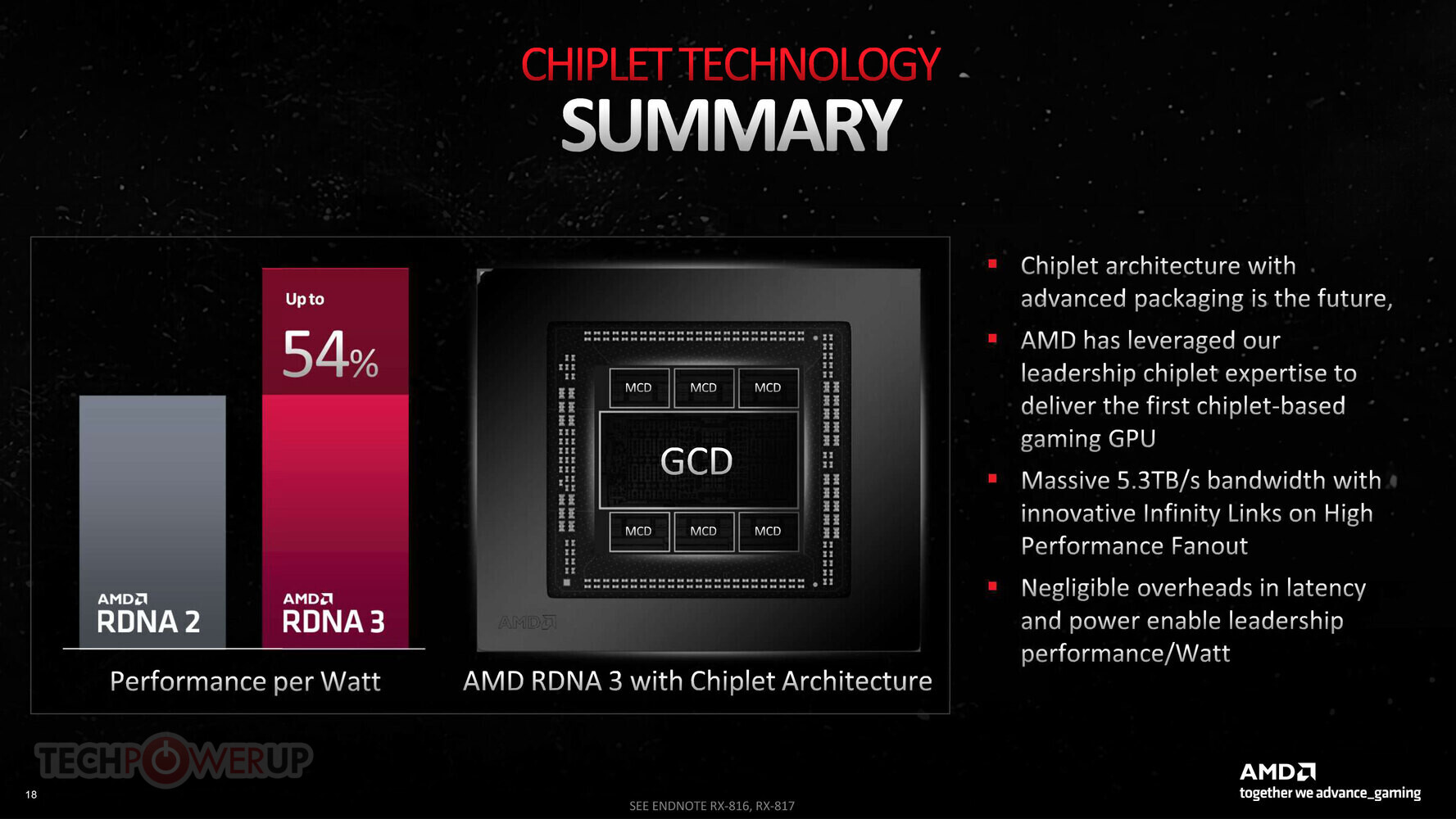
GPUs with memory interfaces wider than 64-bit tend to use multiple 64-bit memory controllers that are interleaved to create a wider memory interface (such as 128-bit, 256-bit, 384-bit, etc). This is the case with both AMD and NVIDIA. AMD hence decided that not only will the memory controllers be spun off, but also each memory controller with a 64-bit memory path, would be its own chiplet, and have a 16 MB segment of the GPU's 96 MB of Infinity Cache memory. This memory controller + cache chiplet would be called the memory-cache die (MCD); while the rest of the GPU with its hardcore logic components that actually benefit from 5 nm EUV, would be nucleated into a larger centralized die called the graphic compute die (GCD). The "Navi 31" GPU has a 384-bit wide GDDR6 memory interface, and so there are six MCDs. Assuming AMD sticks with the chiplet design for even its smaller GPUs, it can simply use a smaller number of the same MCDs to achieve narrower memory interfaces, such as 256-bit (4x MCDs), 192-bit (3x MCDs), or 128-bit (2x MCDs).


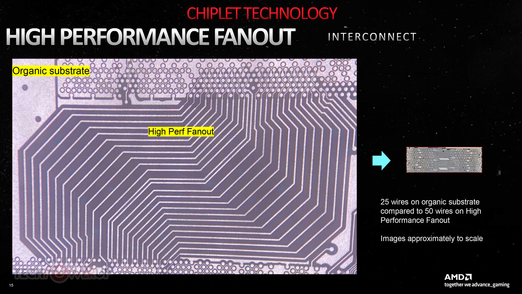
 While the interconnect between the GCD and MCDs is still Infinity Fabric, AMD had to develop a new physical-layer wiring technology that used the existing organic fiberglass substrate, to achieve the kind of high wiring densities needed for thousands of signal paths. The company developed the new Infinity Fanout Link physical-layer, which uses a large number of 9.2 Gbps IF links with fanout wiring, to achieve 10x the wiring density between the GCD and an MCD, in comparison to the IFOP physical-layer used to connect a "Zen" processor CCD with the IOD. A fanout is a technique of achieving a large number of equal-length traces between two points, where putting them in straight lines isn't possible. They are hence made to meander along obstacles (such as vias) in a manner that doesn't compromise the equal trace-length needed to maintain signal integrity.
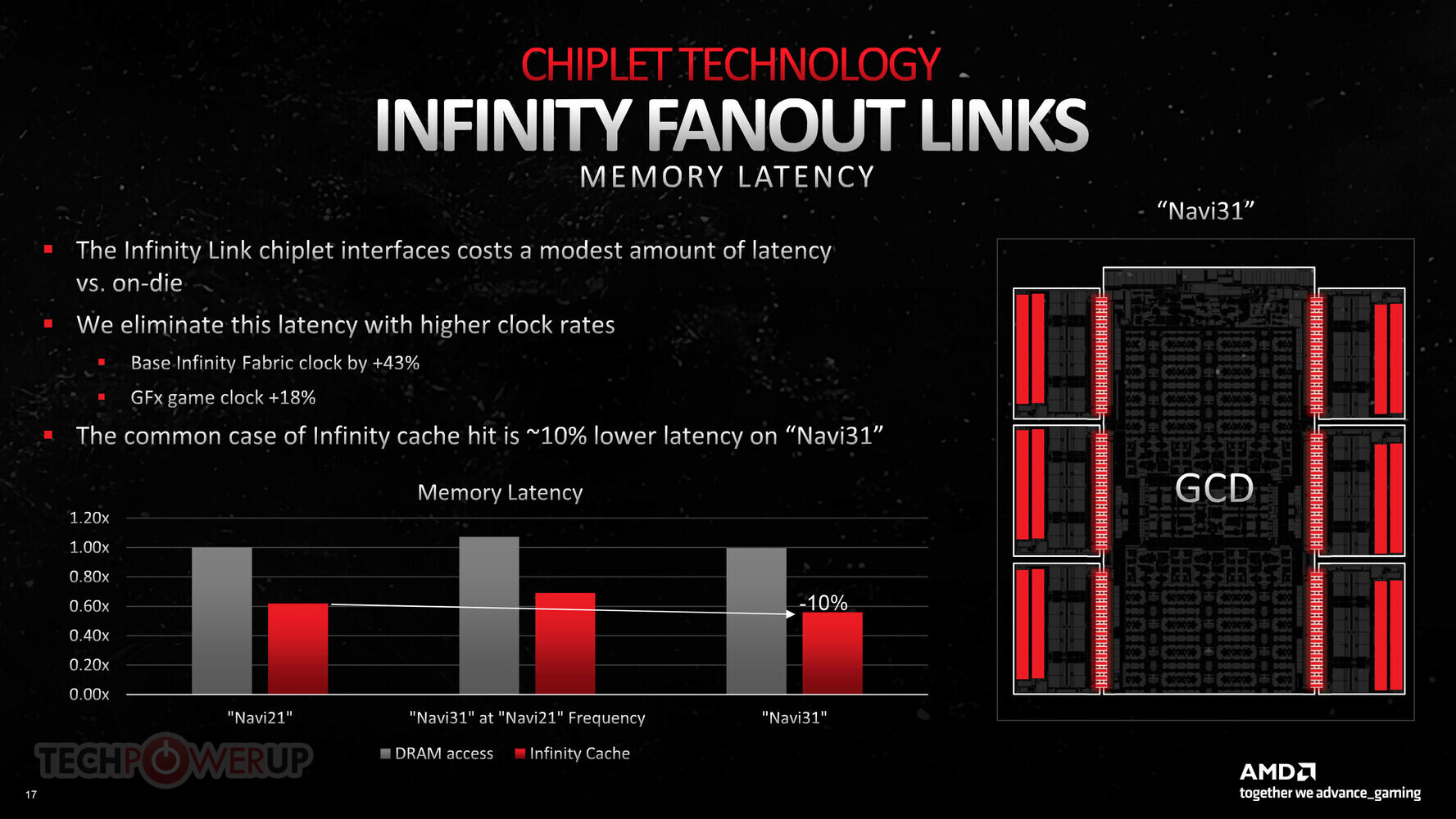
A familiar alternative to AMD for the Infinity Fabric Fanout wiring would have been to use a 3D packaging approach, by using a silicon interposer (a die that facilitates high-density microscopic wiring between dies stacked on top of it). AMD's past MCM GPUs have used interposers to connect the GPU die and HBM stacks. An Interposer is a very expensive way to build a client GPU with headroom for price-cuts in the future, since it's a large 55 nm-class die by itself, which is made to act like a PCB. The obvious downside to disintegrating a monolithic logic chip is latency, which is especially critical for a GPU. While the company doesn't specify it, the spinning off the memory controllers to MCDs have added a "modest amount of" latency as opposed to having them on-die (like on "Navi 21"). AMD says it attempted to overcome this latency by increasing the clock-speeds. The base Infinity Fabric clock is 43% higher than that on the "Navi 21," and the game clocks (shader engine clocks) have increased 18% gen-on-gen. The cumulative bandwidth of the Infinity Fanout links between the six MCDs and the GCD, is 5.4 TB/s. This bandwidth is needed, despite the GPU's overall GDDR6 memory bandwidth only being 960 GB/s (at 20 Gbps reference memory speed); because the MCD also contains a segment of the Infinity Cache, which operates at a much higher data-rate than the GDDR6 memory.
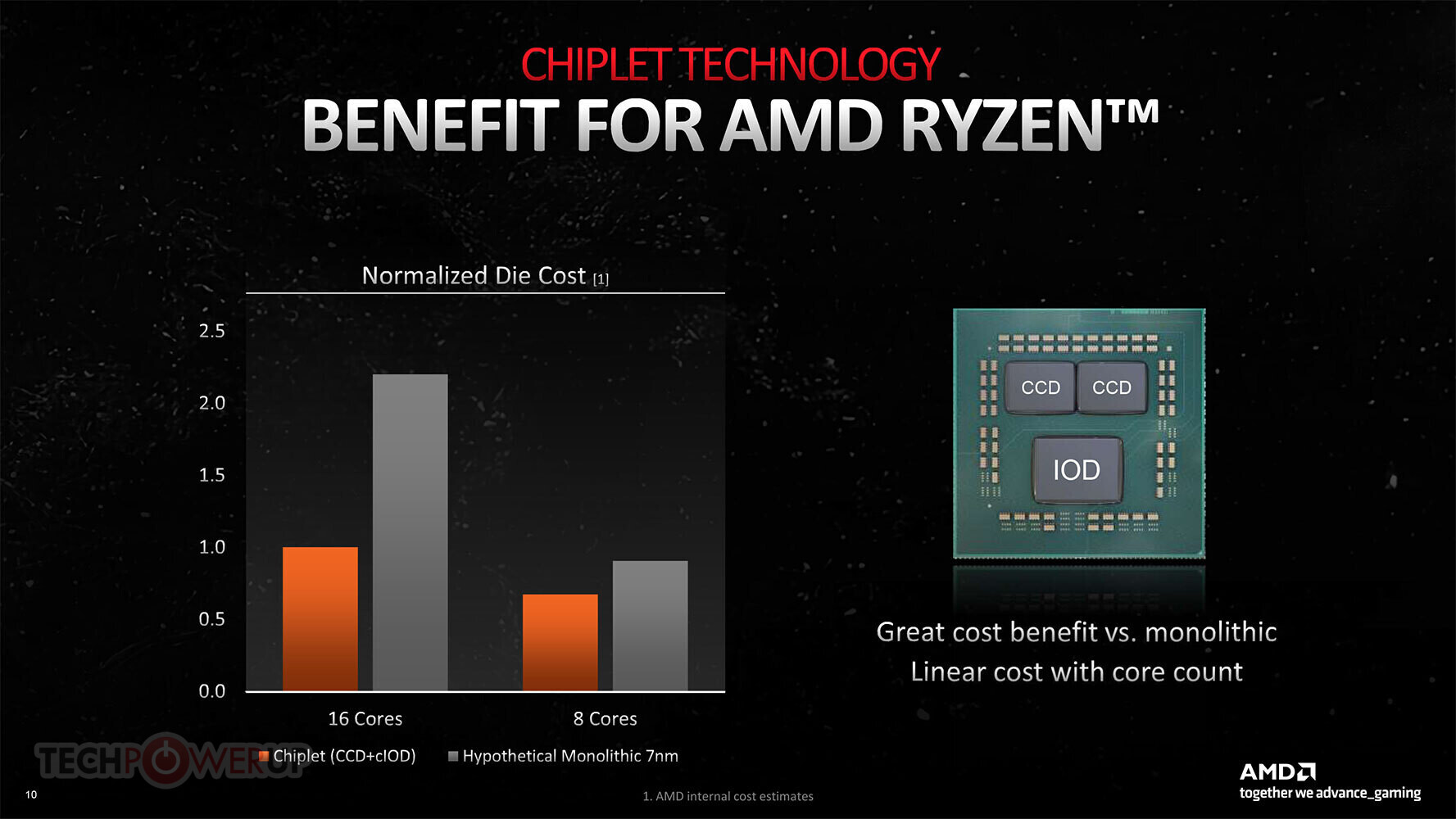
 AMD has also, for the first time, explained the economics of the chiplet approach to building its Ryzen client processors. Were a 16-core Ryzen chip, such as the Ryzen 9 5950X, been built on a monolithic 7 nm die, it would have cost AMD 2.1 times more in comparison to its chiplet-based approach of using two 8-core 80 mm² CCDs paired with a cheaper 12 nm I/O die. Because then the company would've had to build a much larger 7 nm chip with all 16 cores on it, the I/O components; and also suffer lower yields due to the resulting die being larger (in comparison to the tiny CCDs).
An example of an MCM would be a mobile Intel Core processor, in which the CPU die and the PCH die share a substrate. Here, the CPU and the PCH are independent pieces of silicon that can otherwise exist on their own packages (as they do on the desktop platform), but have been paired together on a single substrate to minimize PCB footprint, which is precious on a mobile platform. A chiplet-based device is one where a substrate is made up of multiple dies that cannot otherwise independently exist on their own packages without an impact on inter-die bandwidth or latency. They are essentially what should have been components on a monolithic die, but disintegrated into separate dies built on different semiconductor foundry nodes, with a purely cost-driven motive.


AMD is hardly TSMC's only customer, and the company soon realized that it couldn't make high core-count CPUs on monolithic 7 nm dies; nor could it do what it did with EPYC "Naples," which were basically "4P on a stick" MCMs, with wasted die-space to redundant components. It hence disintegrated the processor. The components that could benefit the most from the shrink to 7 nm; the CPU cores, would be built on tiny dies containing 8 CPU cores each, which the company would call CPU complex dies (CCDs). The smaller the die, the higher the yield per wafer, and so the company decided that a 80 mm²-ish piece of silicon with 8 CPU cores, would talk to a separate die containing all the components that it could afford to build on a slightly older node with minimal impact on the product's overall power/thermal characteristics. It would call this the I/O die. AMD would go on to build both client Ryzen and server EPYC products with this approach, as the 8-core CCDs were common to both product lines. The client desktop processor would have a smaller I/O die suitable to the platform, which it would call cIOD (client I/O die), while the server part, with the ability to connect with a higher number of CCDs, would be called the sIOD (server I/O die). AMD continued to source I/O dies from Globalfoundries, on its 12 nm node, for the past three years. With the latest Ryzen 7000 and 4th Gen EPYC processors based on "Zen 4," AMD is building the CCDs on the 5 nm EUV node, while the I/O dies are built on the less advanced 6 nm node.
Fast forward, and AMD found itself staring at a problem with its Radeon GPUs. The company doesn't make as much money selling discrete GPUs as it does with CPUs (client+server), so the imperative to reduce manufacturing costs is even higher, without losing competitiveness against NVIDIA. With the GeForce "Ada Lovelace," generation, NVIDIA continues to bet on monolithic silicon for GPU, building even its largest "AD102" chip as a classic monolithic GPU. This presents AMD with an opportunity to lower the manufacturing cost of its GPUs, which could enable it to wage price-wars against NVIDIA, in an attempt to gain market-share. A case in point is the relatively aggressive pricing AMD is using for the Radeon RX 7900 XTX, at $999; and the RX 7900 XT at $899, which the company thinks have what it takes to take the fight to NVIDIA's $1,199 RTX 4080 and probably even trade blows with the $1,599 RTX 4090 in some best-case scenarios.
Step one of disintegrating a high-end GPU without hurting its performance, frame-times, and power/thermal characteristics; is to identify the specific components on the silicon that could be spun off into chiplets, that can make do with an older foundry node. For an EPYC server processor, even with 9-12 chiplets, the company only has to deal with hundreds of signal paths traversing the substrate, to interconnect the chiplets. A high-end discrete GPU is a lot more complex, and the scale of these inter-chiplet signal paths number in the thousands (in case of the older "Navi 21" RDNA2 silicon). With the larger "Navi 31" RDNA3, this count is only going to be higher. The company identified the components that made up at least one-third of the die-area that wouldn't benefit tangibly from the switch to 5 nm EUV—these would be the GDDR6 memory controllers, memory PHY, and the Infinity Cache memory (the GPU's L3 cache shared among all Shader Engines).
GPUs with memory interfaces wider than 64-bit tend to use multiple 64-bit memory controllers that are interleaved to create a wider memory interface (such as 128-bit, 256-bit, 384-bit, etc). This is the case with both AMD and NVIDIA. AMD hence decided that not only will the memory controllers be spun off, but also each memory controller with a 64-bit memory path, would be its own chiplet, and have a 16 MB segment of the GPU's 96 MB of Infinity Cache memory. This memory controller + cache chiplet would be called the memory-cache die (MCD); while the rest of the GPU with its hardcore logic components that actually benefit from 5 nm EUV, would be nucleated into a larger centralized die called the graphic compute die (GCD). The "Navi 31" GPU has a 384-bit wide GDDR6 memory interface, and so there are six MCDs. Assuming AMD sticks with the chiplet design for even its smaller GPUs, it can simply use a smaller number of the same MCDs to achieve narrower memory interfaces, such as 256-bit (4x MCDs), 192-bit (3x MCDs), or 128-bit (2x MCDs).


A familiar alternative to AMD for the Infinity Fabric Fanout wiring would have been to use a 3D packaging approach, by using a silicon interposer (a die that facilitates high-density microscopic wiring between dies stacked on top of it). AMD's past MCM GPUs have used interposers to connect the GPU die and HBM stacks. An Interposer is a very expensive way to build a client GPU with headroom for price-cuts in the future, since it's a large 55 nm-class die by itself, which is made to act like a PCB.
19 Comments on AMD Explains the Economics Behind Chiplets for GPUs
Very cool to finally see chiplet GPU done. I remember an Nvidia slide years back. AMD beat them, hard, I wonder what's the counterpunch and how long it'll take.
Everyone's milage does varey so I am not discrediting your Stance, regardless it's not everyone's, though you and others experience has been different to mine and others perhaps.
Thinking the new cpu and gpu with the same 7k numbers is really weird :kookoo:
www.semianalysis.com/p/ada-lovelace-gpus-shows-how-desperatewww.angstronomics.com/p/amds-rdna-3-graphics(please read InFo_OS as I n F o _ O S)